Zettaflops technical report ZF014 v2
Version 1
Zettaflops technical report ZF014 v2
Version 1
This post is about a spreadsheet that computes inductor parameters for the 4LC resonator. There is a download link for the spreadsheet immediately below the the description.
To succeed, reversible logic must beat CMOS as an effective technology for some important applications. Reversible logic circuits can use scaled semiconductor processes to skip over CMOS’s learning curve, but the energy recycling power supply will need to compete with CMOS immediately. This section defines the problem and solves it.
This section converts an example CMOS chip to reversible logic. Generally, the reversible logic literature shows how to replace the logic gates in a scaled CMOS design with reversible gates while roughly retaining interconnection wires and their lengths. A final layout would require a lot of additional engineering, but this section uses the rough layout to estimate the energy density of the converted circuit. We then create an energy recycling power supply meeting the estimated energy density using superconducting inductors, including newly available inductors of HKI material.
We start by considering stored energy. Resonators, including 4LC, move energy back and forth between the circuit’s capacitance and the inductor. The capacitance and operating voltage determine an amount of energy ½CV2. An inductor’s energy is ½LI2, and the inductor must be able to hold ½CV2 energy without excessive loss or exceeding its critical current.
Capacitive energy. Let us estimate the capacitance of a reversible logic chip based on converting an exemplary CMOS chip. This section includes expressions for various design values followed by values. Say the exemplary CMOS chip has area A = 1 cm2, power supply voltage Vdd = 1 V, clock rate fCMOS = 1 GHz, dissipation PCMOS = 100 W, and say it is a processor with 50% “dark silicon” (the latter meaning half the chip is effectively unpowered during normal operation).
The textbook equation for CMOS chip power “P = ½CV2 f” allows computation of a starting point for capacitance Cs = 2PCMOS/ (Vdd2fCMOS) = 2E-7 F. Let us add corrections for the following:
With corrections, C = (.8) (2) (¼) Cs = 8e-8. This will be the rough estimate for this document, which designers should progressively refine as their design matures.
Energy stored in coils and advanced inductors. If a coil inductor appears too weak, the designer could allocate more space or volume per coil, consider a change of materials, consider one of the superconducting options below, or scale back their expectations for a reversible logic system.
High kinetic inductance (HKI) layers are available for some Niobium-based integrated circuits. Inductance in these materials arises from the momentum of charge carriers, which exceeds “geometric” inductance from a magnetic field by an order of magnitude or more. Furthermore, an HKI inductor does not need empty space for the magnetic field’s energy, so a wire’s length solely determines the inductance. These properties allow fabrication of superconducting inductors with lower loss due to the wire’s superconductivity, higher inductance due to HKI, and of multiple layers.
Niobium superconductors operate at about 4 K, although YBCO has similar properties and operates at 77 K (the boiling point of nitrogen). This document applies to YBCO and other high-Tc inductors as well. Some R&D teams are seeking to create high-Tc superconductors with high kinetic inductance.
Other R&D teams seek to create superinductors. An inductor made from a perfect conductor in vacuum has limits due to the properties of vacuum. A “superinductor” is an inductor of any type that exceeds the vacuum limit. Since HKI uses charge carrier momentum rather than a magnetic field, the properties of vacuum are irrelevant, creating a path for HKI superinductors. There are reports of laboratory measurements on HKI inductors that exceed the vacuum limit.
The 4LC hybrid illustrated in Fig. 1 will benefit from advanced inductors and will benefit from superinductors when they become available. The 4LC hybrid comprises an inductor layer and a semiconductor layer, where the inductor layer contains four copies of an inductor. Each inductor interacts with the capacitance of transistors and wires in a reversible logic circuit. So, let us consider a reversible logic circuit of area A interacting with planar HKI superconducting inductors of area A/4.

We can use the properties of a square of material to estimate the properties of an arbitrarily shaped kinetic inductor. Like resistance per square, the value L□ suffices to characterize HKI inductance. The design principle is that squares of material have the same resistance R□ or inductance L□ when measured between opposing sides – irrespective of the length of the side. Of course, lithography defines the minimum length of a side. A designer can estimate inductance similarly to resistance by dividing a shape into a mesh of inductors of value L□ and using the rule for parallel-series interconnection between inductors, which is the same rule as for resistors.
For representative properties, a semiconductor process [2-Yohannes 24] offers HKI with inductance per square L□ = 8.5 pH/□, w = 0.8 µm minimum width, s = 1 µm minimum spacing, and Ic = 2.5 mA/µm = 2,500 A/m critical current. Thus, the current limit of the narrowest allowable wire is Imax = Icw = 2 mA.
If an HKI inductor under consideration does not have enough energy storage capacity, a foundry may be able to create NL layers, which would increase the energy storage capacity by a factor of NL. Adding layers to a chip normally increases cost, mostly due to increasing the number of lithography layers.
However, some integrated circuit fabs produce flash memory chips with hundreds of layers without a lithography step for each layer. A designer could investigate the availability of an NL-layer HKI inductor.
Maximum current. Next, the designer must make an inductor with enough current carrying capacity. A designer could initially select the peak-to-peak sine wave voltage to equal the recommended Vdd for CMOS circuits. The designer could later refine the initial value through simulation to account for differences in the waveforms presented to transistors by CMOS and reversible logic. In the author’s experience, such refinement changes the optimal voltage by about a third.
With a known sine wave voltage, circuit analysis or simulation will reveal the peak inductor current at the desired operating frequency. Wire big enough to handle the peak current, plus an insulating gap, must fit in the space available.
If the inductor is a coil of normal metal, the designer may be able to trade off wire diameter for the number of turns in the coil, but reducing wire diameter increases resistance that will lower the Q factor.
If the inductor is a wire following a planar path made of an HKI superconducting material, the designer can vary the wire width without changing the insulating gap. This will change the maximum or critical current, and may change the energy storage capacity of the inductive layer.
Let us continue our example to give the reader insight into typical values. Say each inductor will occupy a quarter of the exemplary chip in Fig. 7, AL = A/4. Each inductor of area AL, taken as a square, is large enough for (√AL) / (w+s) = 2,780 parallel wires with the required spacing. The total length of wire will be AL/ (w+s) = 13.9 m. Ignoring corners, the wire will be AL/ (w (w+s)) = 17.4 M squares in length hence inductance AL□ / (w (w+s)) = 148 µH. The textbook formula for energy on an inductor “(½LI2)” yields ½AL□ / (w (w+s)) (Ic w)2 = ½AL□ Ic2w / (w+s) = 295 pJ/inductor at maximum current.
Clock regions. The designer now divides the circuit into NR clock regions of equal area. Each such region should have a statistically similar capacitance and hence use a similar amount of power-clock current. If the designer creates a 4LC circuit for each region, each such circuit will have capacitance and peak current reduced by a factor of NR, but inductance increased by NR. All the 4LC regions would receive the same drive waveforms.
While a 4LC circuit maintains the 90˚ phase between clocks, the designer will need to verify that the coupled 4LC circuits maintain phase accurately enough – including in instances where the circuit’s computation causes uneven loads or crosstalk. For example, reversible logic in one region creating and sending signals to another region, which recovers the signal energy, would create a net flow of energy between regions. This flow would be crosstalk.
Fig. 1 shows an inductor, copied once for each clock phase, such that the aggregate area is the same as the reversible logic circuit. Fig. 7c shows capacitance C1 as the wiring for a clock phase and C0 as a lumped capacitor with an “equivalent capacitance.” C2 and C3 receive similar treatment.
At the design level, the result is replicable layout geometry, or reversible logic IP. A designer can lay out multiple units of IP on a chip surface and they will function properly (given proper connections to power, clocks, and external data).
To continue our example, a 4LC circuit with the exemplary capacitance and resistance values resonates at a frequency fqtr = 65.5 KHz, where fqtr is the frequency for a “quarter chip” inductor.
A simple adjustment to the analysis above would allow us to choose the operating frequency, say fR = 100 MHz. We divide the exemplary chip into NR = fR / fqtr = 1,530 regions, yielding LR = L/NR = 96.7 nH and CR = C/NR = 52.4 pF. The energy flux through the capacitor will be ½CRV2 fR NR = 4 W. The inductor’s stored energy is ½LRImax2 = 0.19 pJ and energy flux ½LRImax2 fR NR = 29 mW.
The inductor’s energy storage capacity falls short by 136x. The designer could build a system with NL = 136 HKI inductance layers or change parameters as indicated in section II below.
Getting started. The reader should open the associated spreadsheet 4LCWorksheet.xls. The spreadsheet should open to the first tab called “Worksheet.” Column K contains parameter modifications for design space exploration and column L explains the parameter with text of the form “<- explanation of change.” If the reader sets all the parameter modification factors to 1, the spreadsheet will calculate the values described in the previous section – including the need for 136 HKI layers (which is too many for current technology).
If the reader reopens the file, restoring the original parameter modifications, the computed number of required HKI layers will be 1.002 (essentially 1), indicating a feasible design with current technology. The reader will see that the required changes from the previous section comprised:
Other tabs. The spreadsheet is not a polished application, but sheets 2-4 may be useful as a starting point for further development. The sheets apply to HKI, coil, and meander inductors respectively.
Each sheet computes and plots the energy density of an inductor class. When using a display with 4K resolution, clicking on the tabs for sheets 2-4 displays the power density plot in the same part of the display, allowing the user to compare inductor classes easily.
Sheets 3-4 include spreadsheet formulas for computing inductor parameters, with hyperlinks to source documents on the internet. This document described the HKI inductors used in sheet 2.
Further note on HKI inductor design. It is easy to understand the meander inductors in Fig. 1, yet we can improve this design.
Fig. 2 illustrates an improvement. The reader should first notice that diagram has a center section and a boundary. The scaling concept is that the area of the center section scales quadratically while the boundary scales linearly.

The quadratically scaling center section contains wide wires closely spaced, thus maximizing the energy capacity of the HKI material.
However, making the center section into a meander simplistically would require the charger carriers to navigate “hairpin turns,” which would lead to hotspots or localized areas exceeding the critical current density of the HKI material. Fig. 2 widens wires in turns and reducing the sharpness of turns to avoid such hotspots. The geometric constraint is that the turns cannot be as dense as the wires in the center section. The diagram contains sharp artifacts and extraneous lines from the author’s word processing software that would not be part of a final design.
[1] [1-ZF013] DeBenedictis, Erik. Scaling up Reversible Logic with HKI Superconducting Inductors, Zettaflops LLC technical report number ZF013. https://zettaflops.org/jj-2025/.
[2] [2-Yohannes 24] Yohannes, Daniel, et al. “Materials and methods for fabricating superconducting quantum integrated circuits.” U.S. Patent No. 11,991,935. 21 May 2024. https://patents.google.com/patent/US11991935B2/en.
The text above is from the pdf file below.
Resonators generate sine waves directly, but maintaining a 90˚ relative phase between the power-clocks becomes a challenge. Past work tended to use four independent waveform generators initialized with phases in progressive multiples of 90˚. The phase relationship stayed constant due to precise frequency control or synchronization.
To illustrate the problem, say one of the power-clocks misses its intended frequency by 1 Hz. After ¼ of a second, its waveform will align with one of the neighboring waveforms. This would cause the reversible logic circuits to run incorrectly, potentially in reverse.
The solution would be to find a type of resonator that naturally oscillates as four sine waves with phases in progressive multiples 90˚.
This post introduces the circuit shown in Fig. 1, called 4LC, and derived from the lumped-element transmission line shown in Fig. 1a. Sine waves propagate without loss in both directions up to a maximum frequency or minimum wavelength. Due to its lumped circuit nature, we must measure wavelength in circuit stages rather than distance.

Fig. 1b shows the lumped-element transmission line connected into a cycle. Subject to frequency or wavelength limits, the cyclic circuit will carry periodic waveforms independently in both directions. However, the period of sine waves making up a periodic waveform (i.e. Fourier decomposition) must be an integral fraction of the waveform’s period. The allowable integers are zero and one in the four-stage lumped transmission line. Zero corresponds to DC and one corresponds to a sine wave whose wavelength is four stages.
The lumped transmission line model helped explain properties of the four-stage circuit, but we will subsequently consider the 4LC circuit to be four inductors and four capacitors as illustrated in Fig. 1b. We know from transmission line analysis that 4LC has two oscillation modes, one looking like four-phase power-clocks and the other comprising the same waveforms propagating backwards.
The 4LC circuit has oscillation modes, each characterized by a frequency and an amount of energy. Theoretically, the 4LC circuit is lossless and would oscillate forever. However, losses in the 2LAL circuit cause the total energy to decrease over time, including loss of energy in oscillation modes plus crosstalk between modes.
We now explain the 4LC circuit’s parasitics for completeness. Since the 4LC circuit has eight components, each with one state variable, the modes must span eight degrees of freedom. A general eigenvalue and eigenvector analysis appears in the next section, but circuit symmetries allow a less mathematical solution here.
The reversible logic clocks in each direction have amplitude and phase, consuming four degrees of freedom. A DC offset consumes a fifth (a DC offset of Vp/2 positions the sine wave between GND and Vp). A circulating current in the inductors consumes a sixth (which can be important for superconductor implementations). A parasitic mode discussed below accounts for the remaining two.
Moving the 4LC circuit components to different positions in Fig. 1c reveals a line of symmetry. Due to symmetry, initializing the two halves of the circuit identically would lead to time evolution where the voltages on (P0, P2) and (P1, P3) remain the same forever. Putting wires between nodes that have equal voltages will not alter behavior, so we can turn the dashed lines P0-P2 and P1-P3 into wires and simplify the circuit. Simplification merges four parallel inductors into a single inductor of ¼ the inductance. Four capacitors appear in series-parallel combination that simplifies to a single capacitor. Thus, the circuit’s behavior will be equivalent to an LC circuit with the same capacitance but ¼ the inductance. This mode will oscillate with frequency 2fLC. This parasitic mode has two degrees of freedom representing amplitude and phase. In summary, the frequencies discussed differ by multiples of √2:
The author chose the 4LC circuit by visualizing circuit networks, yet circuit visualization does not reveal certain engineering details. For example, visualization will not reveal the effect of an out-of-tolerance inductor. However, state space analysis reveals such quantitative effects. This section outlines how to obtain additional quantitative detail, but the reader could consult an engineering textbook for further details.
As mentioned previously, an LC circuit has separate degrees of freedom, or independent variables, for the current in each inductor and the voltage on each capacitor. As identified on the top row of the table below, we say xi, i=0…3 is a variable representing the current in inductor Li, and xi+4, i=0…3 is a variable representing the voltage on capacitor Ci. In mathematical notation, a dot over a variable, such as ẋ, represents time derivative, so ẋi, i=0…3 is the time derivative of current xi, so Liẋi is the voltage across inductor Li, based on the equation for voltage across an inductor. Likewise, ẋi+4, i=0…3 is the time derivative of voltage xi+4, and Ciẋi is the current through capacitor Ci.
| x0= I(L0) | x1= I(L1) | x2= I(L2) | x3= I(L3) | x4= V(C0) | x5= V(C1) | x6= V(C2) | x7= V(C3) | |
| L0ẋ0 = | 1x4 | −1x7 | ||||||
| L1ẋ1 = | −1x4 | +1x5 | ||||||
| L2ẋ2 = | −1x5 | +1x6 | ||||||
| L3ẋ3 = | −1x6 | +1x7 | ||||||
| C0ẋ0 = | −1x0 | +1x1 | ||||||
| C1ẋ1 = | −1x1 | +1x2 | ||||||
| C2ẋ2 = | −1x2 | +1x3 | ||||||
| C3ẋ3 = | 1x0 | −1x3 |
Reading across each row in the table yields an equation based on the topology of the 4lc circuit. For example, L0ẋ0 is the voltage across inductor L0, whose ends connect to C3 and C0, so the voltage across the inductor is the C0 voltage x4 minus the C3 voltage x7.
The reader will see that all columns (except the first column, which has row labels) include a 1 or −1 coefficient and a term xi, where i is the column number (minus one, if we count the column of row labels). The coefficients in the table above form the matrix below. The reader should be able to tie the table to a matrix in an engineering textbook.
| 0 | 0 | 0 | 0 | 1 | 0 | 0 | −1 |
| 0 | 0 | 0 | 0 | −1 | 1 | 0 | 0 |
| 0 | 0 | 0 | 0 | 0 | −1 | 1 | 0 |
| 0 | 0 | 0 | 0 | 0 | 0 | −1 | 1 |
| −1 | 1 | 0 | 0 | 0 | 0 | 0 | 0 |
| 0 | −1 | 1 | 0 | 0 | 0 | 0 | 0 |
| 0 | 0 | −1 | 1 | 0 | 0 | 0 | 0 |
| 1 | 0 | 0 | −1 | 0 | 0 | 0 | 0 |
Decomposing the matrix into eigenvalues and eigenvectors is the next step. For this, the reader may use https://matrixcalc.org/vectors.html. The eigenvalues represent the frequency of the eight oscillation modes, of which
Approachable instructions on computing the relevant eigenvalues are as follows. Go to https:/jj-2025-full-text, expand the matrix to 8×8 using the + button, enter the values as shown in Fig 2, then click “singular value decomposition” (SVD).

The result will be four matrices. The third matrix is diagonal and contains the eigenvalues, as shown in Fig. 3.

The eigenvectors are a bit more difficult to decipher, but can be seen in the fourth matrix, as shown in Fig. 4.

Each column contains one oscillation mode, with the current voltages at the top and the four voltages below.
The middle four columns represent the propagating modes. The fifth column contains voltage values (-√2/2, 0, √2/2, 0). Reduced to just negative, 0, positive, the pattern is (-, 0, +, 0), which is the pattern for a negative cosine wave across the four capacitors. The fifth column contains voltage values (0, -√2/2, 0, √2/2), which is a negative sine wave. The third and fourth column just contain initial currents for the inductors.
Since there are four equal eigenvalues, the SVD produces a valid basis set, but not necessarily the basis set we want. So, we have to create combinations of the columns provided by SVD. In this case, the fifth column ± plus or minus the difference between the third and fourth will make the negative cosine wave propagate backward or forward. Similarly, for the sixth column and its negative sine wave. With this combination, we have turned the result of SVD into sine and cosine waves that propagate backwards and forwards.
Note that the output of an SVD algorithm is not uniquely defined when there are duplicated eigenvalues, so a different implementation of the SVD algorithm could produce different values for columns three to six.
The seventh and eighths columns correspond to a zero eigenvalue, or DC values. The seventh column specifies inductors with equal currents, so it is the circulating current. The eighth column specifies capacitors with equal voltages, so it is the DC offset.
The first two columns are the high frequency parasitic. The eigenvalues are sine and cosine waves, which can be considered a sine wave plus phase.
Changing the 1’s in the first row to 1.01 effectively changes the value of L0, leading to slightly different frequencies and waveforms. Likewise for capacitors. Notably, the mathematics shows a change in the overall frequency while maintaining the clock-to-clock phase.
Other circuits are possible. For example, a 12-stage lumped element transmission line could reproduce the 4lc but also allow tailoring of the waveform by adding a third harmonic. At the price of higher complexity in power-clock generation, the tailored waveform could lead to higher energy efficiency from the same circuit.
Abstract—Researchers developed about a dozen semiconductor reversible (or adiabatic) logic chips since the early 1990s, validating circuit designs and proving the concept—but scale up required a further advance. This document shows that cryogenic inductors made of a new High Kinetic Inductance (HKI) material provide the advance. This material can be deposited as an integrated circuit layer, where it has enough energy recycling capacity to power a reversible circuit of the same size. This allows a designer to replicate and scale a complete reversible logic subsystem in accordance with Moore’s law.
Keywords—reversible logic; adiabatic logic; reversible computing; 2LAL; energy recycling power supply; CMOS; power-clocks; resonator; inductor; high kinetic inductance (HKI); YBCO; superinductor; intellectual property (IP)
Reversible logic circuits created with funding from DARPA1 and others used energy recycling to raise the energy efficiency of logic above CMOS levels, yet extending these efficiency gains to the chip level requires a scalable energy recycling power supply for the circuits. With the recent availability of HKI inductors for the power supply, it is now possible to create much more energy efficient quantum computer control chips for operation at 4 K, essentially by replacing the gates in cryo CMOS circuits (e.g. Horse Ridge2) with reversible circuits of higher energy efficiency, thus enabling more qubits before exceeding cryocooler capacity. This opportunity also applies to Read Out Integrated Circuits (ROICs), or sensors with in situ data processing.
HKI inductors now available operate at 4 K and below, but the approach may extend to 77 K using high-Tc superconducting inductors, such as Yttrium barium copper oxide (YBCO).3-4 Thus, this approach may apply to DARPA’s Low Temperature Logic Technology (LTLT) program,5 which is exploring energy efficiency improvements for a broad range of applications in a cryogenic data center.
MIT-LL6 demonstrated a hybrid monolithic foundry process with semiconductors (CMOS) and a Josephson junction process including HKI, while SeeQC7 developed the HKI process used as an example in this document.
As a next step, this document suggests a scale up test of self–contained reversible logic IP (“intellectual property,” which is a term of art in the semiconductor field for chip layout geometry), including CMOS-converted-to-reversible semiconductor circuits as a base and a superconducting layer that includes HKI. This IP would not require an additional energy recycling power supply, but could be AC-powered like three–phase electrical power transmission (but two- or four-phases at a lower voltage and higher frequency).
Multiple units of such IP could be laid out next to each other on a chip, leading to scalability rules similar to integrated circuits—rather than the less attractive scalability rules that apply to 3D structures—as was the case with previous reversible logic projects.
This document uses the result of a recent materials science advance called High Kinetic Inductance (HKI) to make reversible logic scalable. DARPA funded reversible logic in the early 1990s,1 leading to about a dozen projects creating “successful” test chips. While successful, the test chips did not lead to R&D for scale up testing. In retrospect, the problem was that there was no material available at the time that had the required speed, power density, and scalability for an essential component called the energy recycling power supply. With HKI, it is now possible to fabricate scalable hybrid semiconductor-superconductor chips containing both reversible logic and its unique power supply.
The benefit of reversible logic. CMOS operates on DC power, where energy enters a chip on a DC power wire and charges transistor gate capacitance and capacitance between signal wires. When a data value changes, the ½CV2 energy on the capacitance turns into heat within the chip. The CMOS approach therefore turns CV2 energy into heat for every signal change—and signal changes generally correspond to logic operations and are proxies for computational throughput.
The reversible logic approach uses an AC power supply. On the first half of each clock cycle, approximately the same amount of energy (½CV2) used by CMOS enters the chip, but a reversible logic chip returns almost all the energy on the second half of each cycle—thus decreasing wall-power energy consumption by factors in the range of 10x-1,000x.
The HKI advance. Most reversible logic R&D comprises reversible logic circuitry and a separate energy recycling power supply. A semiconductor foundry creates the logic circuit, which is scalable much like a CMOS chip, but the energy recycling power supply relies on a non-scalable component, such as an inductor elsewhere on a printed circuit board or in a 3D structure. In other cases, it is an integrated component, such as a spiral inductor, but which is much larger than the reversible circuitry it supports.
A single layer of HKI inductors has about the same energy density as a cryo semiconductor circuit (CMOS or reversible, which have about the same energy density), thus allowing the non-scalable component in the previous paragraph to become an additional layer right on top of a reversible circuit.
Potential impact. Reversible logic is like a “Moore’s law booster,” meaning it applies to the latest semiconductor process at any point in time, increasing energy efficiency over and above what Moore’s law provides. As such, reversible logic can increase performance within existing power envelopes or reduce power for the given application. Subject to cryogenic operating temperatures, reversible logic applies to applications that would otherwise use the latest version of CMOS.
With today’s technology, reversible logic applies to 4 K cryogenic systems, such as quantum computer control and integrated sensor arrays. There is a future path for high Tc, 77 K operation, such as the DARPA LTLT program.5
Potential scale-up test. This document is not intended as an R&D proposal, but the technology appears ready for a scale-up test comprising the following phases:
This section explains how a High Kinetic Inductance (HKI) material enables reversible logic scale up. For brevity, this document does not describe the underlying principles of reversible logic, but interested readers can read ref. 8.
Background. Athas,1 et. al. created, fabricated, and tested the AC-1 reversible microprocessor in the early 1990s under DARPA sponsorship, demonstrating increased energy efficiency over and above Moore’s law. One might have expected follow-on DARPA scale up testing, but there was none. Instead, other R&D groups tested about a dozen variants of the circuits used in the DARPA project, coining circuit family names such as SQRL,8 2LAL,9-10 RERL,11 S2LAL,12 Q2LAL,13 and others—but the author does not know of any scale up tests. The author’s position is that scale up required a physical science advance, so further circuit testing was destined to yield similar, unscalable results.
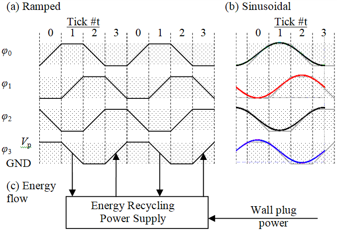
Power-clock background. Reversible logic uses energy recycling, as illustrated in Fig. 1. Past R&D on reversible circuits yielded many logic families, all with ramped 4- or 8-phase clocks. The 4-phase version illustrated in Fig. 1a is for 2LAL.9-10 As illustrated in Fig. 1c for the bottom clock waveform, energy moves into the reversible circuit during the rising edge of the clock. The energy mostly charges gate, wire-to-GND, and wire-to-wire capacitance. The capacitive energy moves back into the energy recycling power supply during the falling edge of the clock, and the cycle repeats using the recycled energy plus a small amount of wall plug power.
The efficiency of the energy recycling process depends on resistive losses in the semiconductor circuit, which rise with clock frequency. Excluding the energy recycling power supply (because this document offers an improvement), the recycling efficiency can be around 90% at the typical clock rate of room-temperature CMOS (~1 GHz), indicating an energy efficiency increase of 10x. At lower speeds, the recycling efficiency may be 99% or higher, corresponding 100x or more.
The ramped clocks in Fig 1a are for the reader’s convenience when accessing the large body of existing literature on reversible logic. In this document, the energy recycling power supply is just inductors, so the natural clocks are the sinusoidal waveforms in Fig. 1b. The reader will see the waveforms have the same basic shape – and the author’s tests indicate they both have about the same energy efficiency when powering reversible circuits.
Scale up story narrative. To understand scale up, we first need a few key facts about the solution in Fig. 2c. The solution will be to cover the reversible logic semiconductor circuitry (bottom) with one or more layers of HKI material (top). Lithographic patterning will divide the HKI material into inductors (shown as meanders) that connect pairs of clock phases through the vertical pillars (the figure is an exploded view; the pillars are of near-zero height). An external non-recycling waveform will drive the clocks, but will draw an order of magnitude less energy from the wall plug than enters the circuit via the pillars. This is the energy efficiency advantage.
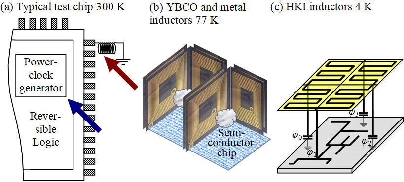
Fig. 2a illustrates a typical scenario for previous R&D efforts.14 An R&D team created a reversible logic test chip as shown, in this case including a “power-clock generator” as identified by a blue arrow. Unfortunately, the R&D team was not funded for scale up testing even though the circuit testing was successful. The red arrow points to the problem, which is a tiny inductor symbol outside the chip. The chip may scale up according to Moore’s law, but the inductor does not. Furthermore, the R&D team did not label the tiny inductor as “future HKI inductor” because HKI material was too new.
Fig. 2b illustrates a higher temperature but more challenging option based on non-HKI (also called non-superconducting or “geometric”) inductors. These inductors require empty space to hold a magnetic field, such as the inside of a coil inductor or free space above and below an on-chip integrated spiral inductor (like the cloud in Fig. 2b). Since it is not possible to deposit “empty space” onto an integrated circuit, Fig. 2b is a 3D structure, which will not scale as well as predicted by Moore’s law.
Fig. 2b shows actual manufactured and tested YBCO inductors. These inductors and their foundry process are close to what is needed for reversible logic, see refs. 3-4 for details. While the 3D structure is not an integrated circuit, there are options for high Tc inductors,15 but they are beyond the scope of this document.
Fig. 2b also applies to normal metal (e.g. room temperature) electrical inductors. Aside from the 3D scalability issues just discussed, normal metal inductors are lossy at high frequencies. Further discussion of normal metal inductors is beyond the scope of this document.
We must now discuss how to implement Fig. 2c and show that an implementation can have sufficient energy capacity at speed.
Converting circuits from CMOS to scalable reversible logic. CMOS and reversible logic circuits are both comprise logic gates and wires, so a designer can replace CMOS logic circuits with the equivalent reversible logic circuits. This is not precisely true, but “true enough” for this argument. The reversible logic layout retains the long wires (e.g. busses) between groups of gates. Based on this imprecise argument, CMOS and reversible circuits will have about the same number of transistors and total wire length—hence the same amount of circuit capacitance and average energy flow during operation.
While the average energy flow rate is the same, the timing differs. Energy enters a CMOS circuit at a constant rate whereas Fig. 1c shows the energy entering the reversible circuit via power-clock φn during tick n (and leaving on tick n+2). The flow pattern for the sinusoidal clocks in Fig. 1b is conceptually the same but less distinct.
Numerically, the 4 mm x 4 mm Horse Ridge cryo CMOS qubit controller2 consumes 10-140 mW, or ECMOS = 62-875 mW/cm2. Based on the text, the range 10-140 mW corresponds to clock rates of f = 100 MHz-1.6 GHz.
The energy capacity per unit area of an HKI material has a simple formula, specifically ½L□Imax2, where L□ is the inductance per square of the process and Imax is the maximum current per unit wire width. (To be clear, cutting a square centimeter of HKI material into wires of 0.1 mm and 0.01 mm width yields inductors with different inductances but nearly the same energy capacity.) For the SeeQC process,7 L□ = 8.5 pH/□, Ic = 2.5 mA/µm = 2500 A/m, so ½LI2 = 0.295 nW/cm2. At f = 1.6 GHz, Ereversible = 472 mW/cm2.
Based on rough numbers above, two layers of HKI inductor will suffice for powering a Horse Ridge-like chip converted to reversible logic.
State-of-the-art data center CPUs and accelerator chips have higher energy density and would require a hundred or more HKI layers. Theoretically, HKI inductors can operate in tall stacks like Flash memory, although tall HKI stacks are not currently manufacturable. HKI material is an active research area, so somebody might discover an HKI material with far higher energy density that would support high performance logic with fewer HKI layers.
Fabricating the necessary structure. Fig. 3 shows the baseline stack. The purple layers in Fig. 3a are an MIT-LL Josephson junction process stack (obtained from the internet) and the blue layers in Fig. 3b are the open source 130 nm Sky130 semiconductor process. After fabricating the semiconductor stack, the foundry planarizes the wafer and adds the superconductor stack using a Back End of Line (BEOL) process. Various foundries claim to have processes that are variants of Fig. 3, including MIT-LL.
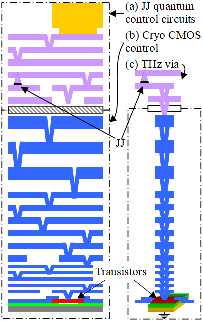
This document does not use Josephson junctions, but just HKI layers and vias, the latter shown in Fig. 3c. It is possible that hybrid chips for scale up testing could use the stack in Fig. 3a, but where an organization interested in Josephson junctions funds the development of the fabrication process. Once the process is available, enterprising chip designers can use it for other use cases, including this one.
Proof of design principle. We now know that HKI inductors have sufficient energy capacity, but we need a “proof of principle” that they will work in a plausible circuit. Fig. 2a needed to minimize the number of external inductors because they limited scalability, but this new design point can have as many lithographically defined inductors as will fit in the available space.
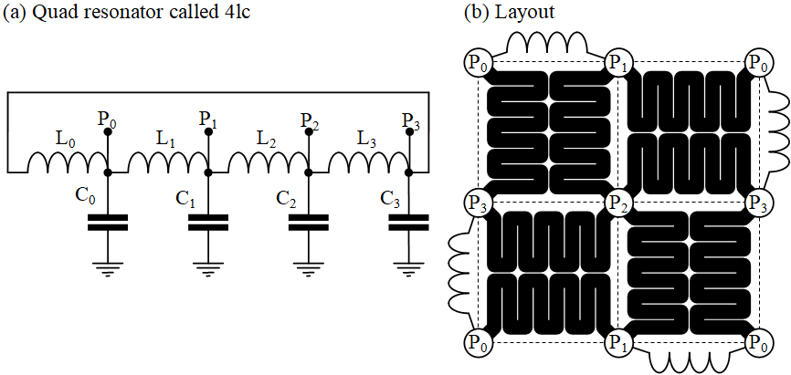
Fig. 4a illustrates the circuit concept, coined 4LC (4-ell-cee), comprising four inductors that naturally oscillate as four sine waves in quadrature as shown in Fig. 1b. Each of the four dotted squares in Fig. 4b effectively contains the circuit in Fig. 4a with each Pn = φn connected to the Cn capacitive loading of the Pn clock for the circuitry within the square. The array can be made as large as necessary, as long as the inductors around the boundary are applied in the pattern shown. The reader will note the absence of synchronization logic, high-current switches, and other complexities. The resonant modes of the LC array perform these functions naturally.
Simulation. The author created a simulation of the 4LC quad resonator in Fig. 4a, with the output appearing in Fig. 5.
For each plot in Fig. 5, the author entered the 4LC circuit into a circuit simulator, using initial conditions to create the sine waves in quadrature shown in Fig. 1b. The author then connected a 2LAL9-10 reversible logic circuit to the sine waves, and found that the circuits would initially function properly. The circuit’s function is to produce eight-phase clocks (as needed for several other reversible logic families), which are initially clean waveforms in the plots.
The 4LC circuit has oscillation modes, each characterized by a frequency and an amount of energy. Theoretically, the 4LC circuit is lossless and would oscillate forever. However, losses in the 2LAL circuit cause the total energy to decrease over time, including loss of energy in oscillation modes plus crosstalk between modes.
If the inductors and capacitors have low loss (i.e. the 4LC resonator has high Q), the circuit simulator will power the reversible logic for some time based on energy provided by the simulator’s initial conditions. The energy will decline over time, resulting in less amplitude in the sine waves and waveform distortion due to crosstalk. The “sine wave overlays” in Fig. 5a have two curves, the 4LC output values Pn and a simulator-generated reference wave. The reader can see the Pn amplitudes decline over time. As called out by the text “fails due to inadequate power” in Fig. 5a, the reversible logic circuit eventually produces a DC voltage. The remedy is to use external power to “top off” the energy in the desired oscillation mode while “draining out” undesired oscillation modes.
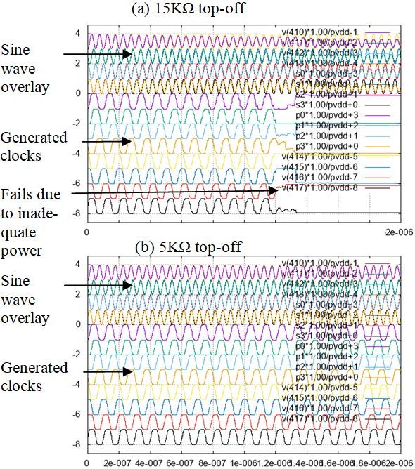
One way to “top off” the 4LC circuit would be to connect conventional sine waves, like those used in three-phase AC power, to the circuit through a resistor. The idea is that the resistor would transfer energy in or out of each oscillating mode until it matches the drive waveform’s amplitude and phase. This includes topping off the desired mode and draining the energy from other modes. The first plot in Fig. 5a uses a 15 KΩ drive resistor, but the resistor was too weak and the circuit failed. However, the second plot in Fig. 5b uses a stronger 5 KΩ resistor, topping off the circuit adequately and yielding consistent sine waves and eight-phase clocks across the chart.
The author used two forms of AC power. The first form was four-phase AC power (shown in Fig. 1a). The second form was two-phase AC power, with phases 90̊ from each other. The two-phase version requires just three wires, GND and the two phases.
Summary. Reversible logic has a long history, but progress stalled due to a missing but necessary physical science advance. This document explains the advance and suggests the time is right for scale up testing.
The document showed how a cryo CMOS-translated-to-reversible-logic circuit and one or two layers of HKI inductor, both of the same area, have about the same energy content and jointly form an energy-recycling power supply. Since the resulting structure is entirely defined by chip layout geometry for a hybrid process, the result scales as predicted by Moore’s law.
The document described and simulated a circuit called 4LC, which creates the four-phase energy recycling clocks used by 2LAL.9-10 A non-energy recycling AC power waveform drives the 4LC.
With today’s technology, reversible logic should be practical for 4 K cryogenic systems, such as quantum computer control and integrated sensor arrays. There is a future path for high Tc, 77 K operation, such as the LTLT program.
The author has two additional files. If this publication (arXiv?) supports supplementary data, it will be added to this paper. The two files are:
A spreadsheet with equations for the top-level planning of reversible logic IP based on properties of the initial CMOS circuit and HKI parameters such as L□, Imax, and lithographic minimums for the width and space between HKI features. The spreadsheet explains how to scale the layout in Fig. 4b so the reversible logic operates at a specific clock rate—a topic not addressed in this document.
The ngspice simulation script that generated Fig. 5.
1. Athas, William C. “Energy-recovery CMOS.” Low Power Design Methodologies. Boston, MA: Springer US, 1996.
2. Pellerano, Stefano, et al. “Cryogenic CMOS for Qubit Control and Readout.” 2022 IEEE Custom Integrated Circuits Conference (CICC). IEEE, 2022. DOI: https://doi.org/10.1109/CICC53496.2022.9772841 https://pure.tudelft.nl/ws/portalfiles/portal/122719163/Cryogenic_CMOS_for_Qubit_Control_and_ReadoutTaverne.pdf.
3. Brandl, Matthias F., et al. “Cryogenic resonator design for trapped ion experiments in Paul traps.” Applied Physics B 122 (2016): 1-9. https://link.springer.com/content/pdf/10.1007/s00340-016-6430-z.pdf https://arxiv.org/abs/1601.06699.
4. Brandl, Matthias F., et al. “Innsbruck high-temperature superconducting resonator.” https://www.traphub.org/electronics/high_temperature_superconducting_resonator_ibk/ibk_hts_resonator.html.
5. Low Temperature Logic Technology, web page https://www.darpa.mil/research/programs/low-temperature-logic-technology
6. Superconducting integrated circuits, web page https://www.ll.mit.edu/research-and-development/advanced-technology/microsystems-prototyping-foundry/superconducting
7. Yohannes, Daniel, et al. “Materials and methods for fabricating superconducting quantum integrated circuits.” U.S. Patent No. 11,991,935. 21 May 2024. https://patents.google.com/patent/US11991935B2/en.
8. Frank, Michael Patrick, and Thomas F. Knight Jr. Reversibility for efficient computing. Diss. Massachusetts Institute of Technology, Dept. of Electrical Engineering and Computer Science, 1999. https://dspace.mit.edu/handle/1721.1/9464.
9. Athas, W. C., et al. “A framework for practical low-power digital CMOS systems using adiabatic-switching principles.” International Workshop on Low Power Design. 1994.
10. Anantharam, Venkiteswaran, et al. “Driving Fully-Adiabatic Logic Circuits Using Custom High-Q MEMS Resonators.” ESA/VLSI. 2004. https://citeseerx.ist.psu.edu/document?repid=rep1&type=pdf&doi=7c8d654ce333d5b032af809c4c7770a61fb3add9
11. Lim, Joonho, Dong-Gyu Kim, and Soo-Ik Chae. “Reversible energy recovery logic circuits and its 8-phase clocked power generator for ultra-low-power applications.” IEICE transactions on electronics 82.4 (1999): 646-653. https://s-space.snu.ac.kr/bitstream/10371/21101/1/Reversible%20Energy%20Recovery%20logic%20circuits%20and%20its%208-phase%20clocked%20power%20generator%20for%20ultra-low-power%20applications.pdf.
12. Frank, Michael P., et al. “Reversible computing with fast, fully static, fully adiabatic CMOS.” https://doi.org/10.1109/ICRC2020.2020.00014 2020 International Conference on Rebooting Computing (ICRC). IEEE, 2020. https://arxiv.org/pdf/2009.00448.
13. DeBenedictis, Erik. “Managing energy in computation with reversible circuits.” U.S. Patent Application No. 18/282,035. https://patents.google.com/patent/US20240152175A1/en.
14. Kim, Suhwan, Conrad H. Ziesler, and Marios C. Papaefthymiou. “A true single-phase 8-bit adiabatic multiplier.” Proceedings of the 38th annual Design Automation Conference. 2001.
15. Srivastava, Yogesh Kumar, et al. “The elusive high-Tc superinductor.” arXiv preprint arXiv:2209.01342 (2022). https://arxiv.org/pdf/2209.01342.
The file below is a slide deck presented at the USC4SCE “JJ” workshop in Santa Fe, NM on April 10, 2025.
Zettaflops LLC technical report ZF013 accompanies the presentation and appears below. An inline version appears in a concurrent post. The document is also available via arXiv at https://arxiv.org/abs/2504.09229.
I have uploaded a very brief document on optimizing several families of reversible circuits.
Original version
Some of my colleagues have expressed interest in the sizing of transistors in reversible logic, so I am posting the result of some simulations I performed in late 2021.
I am posting a PowerPoint at the bottom of this page with simulation output and an explanation. The file is intended to be viewed as an build-up type animation that shows the effect of widening transistors.
CMOS design first and foremost widens transistors to meet timing closure.
Reversible circuits are supposed to be low power, so the baseline assumption is that you should use minimum size transistors everywhere. Such a reversible circuit all will function correctly, but it will not have the lowest dissipation because drops across some of the small transistors will have quadratically growing V2/R losses. So, the lowest energy solution involves making some transistors wider.
Reversible circuits need wider transistors in about the same places as CMOS circuits, namely when driving large capacitive loads or long wires. However, the large transistors reduce dissipation rather than maximize speed. There is an optimal size for both reversible and CMOS transistors, which is where the gate capacitance is about equal to wire capacitance. Gate capacitance larger than this amount causes CMOS to run slower and reversible to dissipate more.
Device variance will cause a reversible gate to dissipate more than the expected amount, but it will still function correctly. This is a better outcome than variance causing a CMOS gate to become slower than expected, miss the setup time of the next latch, and cause data corruption.
The PowerPoint below shows the dissipation of a shift register with a 10 fF wire load. Transistor width is 360 nm, 720 nm, 1.44 μm, 2.88, and μm 5.76 μm. One sees that the reversible advantages shifts to a higher frequency as the transistor becomes wider.
If you would like to contribute to reversible computing, why don’t you make a chip?
There many academic papers describing reversible logic circuit families, the results of circuit simulations, and sometimes measurements of fabricated chips. Making a chip used to require a project with a million-dollar (USD) budget and was further inaccessible to individuals and small groups because commercial semiconductor fabs required Non-Disclosure Agreements (NDAs).
Yet, the Sky130 open-source chip design program https://github.com/google/skywater-pdk emerged in the last couple years that allows anybody with internet access and a laptop to design a chip. Fabbing the design is possible through a Google/SkyWater free multi-project wafer fab https://www.skywatertechnology.com/mpw/open-source-mpw-program/. Basic testing should be possible with readily available lab equipment.
Let me describe what I did over a period of a couple weeks. Individuals and small groups can make important innovative contributions to technology at certain phases of development. So, I tried to see what I could do from an office in an extra bedroom in my house and with a handful of Windows 10/11 PCs. Having worked in the field for some time, my experience is not representative of a new entrant, but I wanted to demonstrate setting up the open-source tool chain to become an effective platform for reversible computing R&D.
I devised the reversible logic family Q2LAL [DeBenedictis 21], [DeBenedictis 22] about a year ago and it had never been subject to intensive engineering analysis or physical testing, so it seemed like a good starting point. The basic replication unit in Q2LAL is an adiabatic amplifier followed by a transmission gate, illustrated in [DeBenedictis 21, Fig. 3 and 4c]. The circuit ultimately has to be lain out in arrays that effectively exploit symmetries inscrutably buried in the circuit structure. Fig. 1 is my second attempt at a layout planning. It is in an ad hoc format that I found convenient and which I will use for explanation.

The top quarter, outlined by a dotted gray rectangle with Âi-1 on the left and Q̂i on the right, has six transistors organized in a row. Each transistor is represented by the schematic symbol for a transistor (identifiable as a short vertical red line). The four transistors on the left of each row comprise an adiabatic amplifier [DeBenedictis 21, left side of Fig. 4c] and the two on the right are a transmission gate [DeBenedictis 21, small rectangle in Fig. 3b].
I created the layout in Fig. 2 using Magic, a tool in the open PDK. For the reader’s orientation, the six transistors in each row of Fig. 1 each correspond to a red (vertical) rectangle crossing a wider green or orange horizontal region. The vertical power and clock lines were not present at this point.

I created the layout in Fig. 2 with Fig. 1 visible in one window of a PC and the Magic workspace in a second window, going back and forth between the two until I could make a layout that was both compact and satisfied the constraints.
Q2LAL has dual-rail signaling, with the second-from-the-top gray rectangle in Fig. 1 processing the – rail [DeBenedictis 21, right side of Fig. 4c]. The circuits need signals from both rails, leading to the crossover between  and – signals in the top two quarters of Fig. 1. The top two quarters are flipped vertically with respect to accommodate the crossover (and likewise for the third and fourth quarters).
Q2LAL circuits compute in the forward direction and recover energy in the reverse direction. Energy recovery uses the circuit in the top two quarters, but horizontally flipped. Thus, the bottom half of Fig. 1 was created by flipping the graphic of the top half in Microsoft Word.
The entire structure in Fig. 1 must be designed so it can be replicated both horizontally and vertically. Horizontal replication controls the length of the shift register and vertical replication increases the word-width of the stored information.
Replication leads to geometric constraints. For example, the vertical blue (metal) lines would carry power (V), ground (G) and various clock phases φ to all the circuits in a column. But there is a complication. The circuit has one set of wires for the even-numbered circuits and another for the odd-numbered circuits. Thus, the symmetries of circuit must cause extension of each blue line to line up with a gap in the circuit above and below. This is easily seen to be true, but creating the layout required solving a puzzle.
I thus enhanced the layout in Fig. 2 to accommodate arrays, yielding Fig. 3.

Fig. 4 shows four copies of the layout in Fig. 3 in a stack with the following orientation changes:
This yields a Q2LAL stage, such as the left or right half of [DeBenedictis 21, Fig. 3b]. An experienced designer will see that I have not fully mastered Sky130 and Magic.

The next step was to integrate the layout with the Q2LAL ngspice simulations discussed elsewhere on this site (https://revcomp.org/q2lal/). Much of the dissipation in integrated circuits is due to the wires rather than the transistors, so simulation of the layout with wire capacitance would tend to validate the advantage of reversible computing over CMOS.
Unlike academic papers where schematics are created with just thinking, layouts like Fig. 2 can be automatically “extracted” to yield a netlist such as the one below. The netlist is pretty much what a designer would create manually for an academic paper and it can be verified as correct in a few minutes through examination.
* SPICE3 file created from q2v13.ext - technology: sky130A

.subckt q2v13
X0 G ck T G sky130_fd_pr__nfet_01v8 ad=4.65e+11p pd=3.9e+06u as=1.28e+12p ps=1.07e+07u w=450000u l=150000u
X1 T -A G G sky130_fd_pr__nfet_01v8 ad=0p pd=0u as=0p ps=0u w=450000u l=150000u
X2 T A phi0 G sky130_fd_pr__nfet_01v8 ad=0p pd=0u as=2.7e+11p ps=2.1e+06u w=450000u l=150000u
X3 -Q phi3 T Vp sky130_fd_pr__pfet_01v8 ad=2.25e+11p pd=1.9e+06u as=2.7e+11p ps=2.1e+06u w=450000u l=150000u
X4 -Q phi7 T G sky130_fd_pr__nfet_01v8 ad=4.075e+11p pd=3.6e+06u as=0p ps=0u w=450000u l=150000u
X5 T -A phi0 Vp sky130_fd_pr__pfet_01v8 ad=0p pd=0u as=2.25e+11p ps=1.9e+06u w=450000u l=150000u
.ends
However, design tools can also extract information about wires, such as length, resistance, and capacitance. This information is human readable, but understanding the impact on performance, dissipation, etc. requires circuit simulation. For example, the underlined portion of the excerpt below (starting with “cap”) gives the capacitance between pairs of wires φ0 and –Q.
timestamp 1651599653
version 8.3
tech sky130A
style ngspice()
scale 1000 1 500000
resistclasses 4400000 2200000 950000 3050000 120000 197000 114000 191000 120000 197000 114000 191000 48200 319800 2000000 48200 48200 12800 125 125 47 47 29 5
parameters sky130_fd_pr__nfet_01v8 l=l w=w a1=as p1=ps a2=ad p2=pd
parameters sky130_fd_pr__pfet_01v8 l=l w=w a1=as p1=ps a2=ad p2=pd
node "T" 3028 286.743 -80 40 ndif 0 0 0 0 0 0 0 0 51200 2140 10800 420 0 0 0 0 0 0 0 0 0 0 0 0 0 0 0 0 0 0 0 0 0 0 50400 2360 0 0 0 0 0 0 0 0 0 0 0 0
[snip]
cap "phi0" "-Q" 30.2468
cap "-A" "ck" 13.56
[snip]
device msubckt sky130_fd_pr__nfet_01v8 1000 40 1001 41 l=30 w=90 "G" "phi7" 60 0 "T" 90 0 "-Q" 90 0
[snip]
Obtaining this information requires a test layout of the circuit so wire geometry is known and can be subject to a numerical assessment of how close the wires come to each other. Some circuits have more internal interconnectivity than other circuits, which leads to denser wiring with more crosstalk that ultimately reduces speed and increases power. These issues are inherent to any design process, but can be controlled with tools such as those that produced the diagrams in this document.
So, here is the unexpected and somewhat untidy story. The English description used a hierarchy of (1) dual-rail adiabatic amplifier [DeBenedictis 21, Fig. 4c] (2) dual-rail adiabatic amplifier+latch (3) bi-directional stage [DeBenedictis 21, Fig. 3b], but the layout was constructed as (1) adiabatic amplifier+latch+wire flyovers, Fig. 3 (2) dual-rail (3) bidirectional stage using wire flyovers, Fig. 4. So, I had to substantially rewire the sQ2.cir file to support the different hierarchy. The result is sQ130.cir in the repository. Note that sQ130.cir has more functions than the layout because it includes a test harness, creates plots, etc.
I then took the .spice file with parasitic extraction that Magic created and manually pasted the capacitance values into sQ130.cir. I included .if (0)-type lines so I could compare the dissipation with and without the parasitics. The results were 1.99532E-14 and 6.02372E-15 J with parasitics on and off.
I fulfilled my objective of validating the suitability of the open-source design flow, although I did not carry this specific project to an R&D milestone.
If I were to proceed as an individual, it would take me another couple months to make a test design that would contribute to the field (such as the note-note design https://revcomp.org/note-note/). The test design could be fabricated with the Google-subsidized multi-project wafer service, which has about a four-month turn-around time. After chips come back, testing is possible with readily available lab equipment – although some more exotic testing (cryo?) would take a lot of specialized equipment.
In a very brief summary, I loaded the Docker version of the SkyWater Open Source PDK https://github.com/google/skywater-pdk on several Windows 10 and 11 laptops in my office. I have general knowledge of IC design from a university class, but the YouTube video Creating a Hierarchical Layout in Magic Using the Sky130 PDK [bminch 21] is a tutorial that describes commands specific to the Magic open sources.
The Github repository is not fully set up at the moment.
The Magic files are QAAmp11.mag, QLatch.mag, and QPhase.mag available at https://github.com/erikdebenedictis/Shift. The Github repository is not fully set up and this information may change.
An earlier version of the Magic data files can be downloaded with the links below. Due web page limitations, the file name extension has been changed from .mag to .txt. You will need to change the file names back to .mag, after which they can be loaded into the Magic tool.
I recommend the approach above for students and hobbyists. You can make a difference even with modest resources.
There is enough promise and opportunity in reversible computing that larger organizations and funding agencies are ponying up real R&D money. Such organizations and the people in them can perhaps take inspiration from this article and realize that the entry point may be lower than it was a few years ago.
[DeBenedictis 21] Quiet 2-Level Adiabatic Logic. Zettaflops, LLC Technical Report ZF009 https://ar.zettaflops.org/CATC/Q2LAL.pdf
[DeBenedictis 22] Q2LAL page on this website https://revcomp.org/Q2LAL.
[bminch 21] bminch. Creating a Hierarchical Layout in Magic Using the Sky130 PDK, https://www.youtube.com/watch?v=RPppaGdjbj0
High performance adiabatic computing systems will need an engineered powertrain, which will be new technology given that current adiabatic demonstrations are too small to reveal important issues. This will be true even if the high performance computer is a quantum computer.
Todays high performance computing systems dissipate around 200 W per chip. For high performance computers, the objective is more performance for the same 200 W per chip, not lower power chips.
Reversible circuits use multiple AC power-clocks. If the chip is running at 200 W per chip, the power-clock generators will need to be far enough away from the chip to avoid excessive dissipation in a small volume causing cooling difficulties. Hence, a separation will be required between the power-clock generators and the chip, as shown in the figure below.

CMOS microprocessors require clock waveforms to be generated within a few centimeters of the chip to avoid waveform distortion. However, reversible systems send power over the AC power-clock conductors, which carry a lot of power hence require a larger separation than just microprocessor clock lines. In conjunction with requirements for a precise waveforms, both classical and quantum system analyses [ZF008] indicate that the power-clock conductors are long enough that transmission line effects need to be considered, i. e. characteristic impedance and reflections.
In summary, document [ZF008] describes how the power-clock generators must launch predistorted power-clocks into the transmission lines such that they arrive the with the desired waveform.
Document [ZF008] also describes how the load presented by the chip affects the proper predistortion, and how different circuit families and design techniques can reduce load variance. Some design techniques inevitably case load variance, such as turning clocks to unused portions of the circuit on and off. The document describes how power-clock generators can change their predistorted waveform in anticipation of changes in chip load.
The page http://revcomp.org/optimal-ramps further describes how the linear ramp waveform frequently found in the literature is a good starting point but the lowest dissipation shape is flatter in the middle (an “s” shape). The overall result is that predistortion needs to be applied to the “s” shape, not a linear ramp.
The a single shift register stage places very little loading on a 50 Ohm coax and produces little distortion. While a single shift register stage may be easy to simulate in Spice, it is not representative of a high performance computer. Scaling the shift register length to 5,000 stages is more representative of a scaled up system, but the circuit is too big for Spice simulation. To address these issues, the script in appendix of [ZF008] scales transmission line parameters. Multiplying the characteristic impedance by 5,000 in a Spice simulation model yields the same voltage waveform as multiplying the number of shift register stages. See [ZF008] for details.
The script in [ZF008] simulates driving a circuit with predistortion to compensate for transmission line distortion.
Say you are tasked to make an ASIC for a computational accelerator and you have the ability to create a CMOS chip that can dissipate 200 W. The task is to asses the feasibility using reversible logic circuits, yet still using the same CMOS process. Based on the figure above, say the power-clocks will drive 2,000 W into the chip of which 1,800 W comes out. That leaves the 200 W dissipation, so you will not have to change the chip’s cooling.
First, engineer the power-clocks and figure out how to cool them. This will give an estimate of the volume required by the power-clock generators and 2,000 W of heat exchangers. This will then give an idea of how long the cables will be and hence the impact of cable RF losses and reflections. Then figure out the predistorted waveform, starting with the objective of a predistortion to yield a linear ramp and then a predistortion for an optimized waveform.
The second topic is to repeat the task above for a 4 K stage in a quantum computer. Say the quantum computer needs a 1 MHz clock, which will determine the fraction of energy dissipated versus ejected. From this, engineer room-temperature power-clocks and the wiring to get the signals to the 4 K stage. This wiring will be longer than the previous example because they will have to pass through a cryostat boundary. Include filtering for extra credit. Figure out the predistorted waveform for both linear optimized waveforms at the chip.
[ZF008] Erik DeBenedictis. Energy Management for Adiabatic Circuits. Zettaflops, LLC Technical Report ZF008, v1.2, April 15, 2021 https://www.debenedictis.org/erik/CATC/EMgt4Adia-ZF008-v1.2.pdf.
Additional information
The literature almost universally depicts reversible logic clocks with linear rising and falling segments, yet ramps that are flatter in the middle dissipate less. The reason for linear ramps that the simplest explanation of adiabatic behavior assumes transistors have a fixed Ron when conducting, and linear ramps have the lowest dissipation when Ron is constant. The simplest explanation is given first.
Ron actually decreases with larger forward bias on the gate, and behavior is further complicated by saturation. The lowest forward bias is at the middle of the swing, or the midpoint of the ramp.
In simple terms, the best waveform rises quickly when the transistor is on strongly or off, but needs to slow down when the resistance is higher to avoid I2R losses.
Ramps are described in this software as having unit width and height, so the baseline linear ramp goes from (t=0, v=0) to (t=1, v=1). Pretty good ramps can be created by dividing the unit time into five linear sub ramps of length .2. With two parameters, h1 and h2 (h for height), the segmented ramp will go through the following points: (t=0, v=0), (t=.2, v=h1), (t=.4, v=h2), (t=.6, h=1-h2), (t=.8, h=1-h1), (t=1, v=1).
In developing software on this site, it was found that dissipation can be reduced by around 30% through proper ramp shape, with 5 segments adequate to get within about 1% of optimal.
For many circuits, the parameters o1=.20 h1=.34 o2=.40 h2=.46 are a good starting point. H1 and h2 can be fine tuned by optimization. For additional generality, the time divisions are defined by statements o1=.2 and o2=.4 (o for offset), although this is not necessary in most cases..